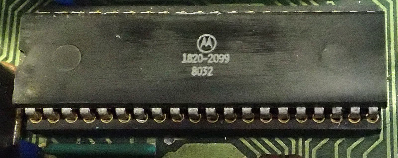
Motorola 1820-2099 – HP-engineered 6802 CPU, with on-chip clock and internal RAM with a retainable section
The Motorola 1820-2099 is a 6802-class CPU engineered and built by Motorola for Hewlett-Packard. It is a variant aimed at embedded and instrumentation systems, where reducing external components (integrated clock and on-chip RAM) and maintaining software compatibility with the 6800/6802 ecosystem enable compact and reliable platforms.
Practically, it is an 8-bit CPU with 16-bit addressing and the ability to build systems up to 64K of addressable space, with internal RAM suitable for critical variables, stack, and small buffers, plus a “retainable” RAM portion that can be preserved under specific operating conditions.

On-chip clock: integration and reduced component count
On-chip clock circuit
The integrated clock circuit reduces the need for external logic to generate/condition the clock signal. In practice:
The BOM is simplified (fewer components).
Failure points and timing variability are reduced.
It is easier to build compact boards for instrumentation and control.
On-chip RAM: 128 × 8-bit and a 32-byte retainable area
128 × 8 bit on-chip RAM
The CPU integrates 128 bytes of internal RAM. Operationally, this allows:
32 bytes of RAM are retainable
A 32-byte portion is specified as retainable. Practically, this feature is useful for preserving a minimal state (flags, counters, parameters) when the main supply or the system goes through specific modes, depending on platform design and any power/backup handling.
Software compatibility: EF6800 and ecosystem continuity
Software compatible with the EF6800
Software compatibility with the EF6800 means the programming model and instruction set remain consistent with the 6800 lineage. In practical terms:
Firmware porting is easier from 6800-derived systems.
Existing toolchains, assembly libraries, and established design patterns can be reused.
Expandability and memory space: up to 64K
Expandable to 64K words
The CPU supports expansion up to 64K addressable space via 16-bit memory addressing. In practice:
I/O and interfacing: TTL compatibility
Standard TTL-compatible inputs and outputs
TTL-compatible inputs/outputs simplify interfacing with standard logic and peripherals of the era. In practice:
Integration with latches, decoders, drivers, parallel buses, and “classic” peripherals is easier without complex level shifting.
Word size and addressing: 8-bit data with 16-bit addressing
8 bit word size
The native data width is 8-bit, so most arithmetic/logic operations are optimized for bytes.
16 bit memory addressing
16-bit addressing enables up to 64 KB memory mapping, consistent with the stated expandability.
Practically, the memory map and decoding design (ROM/RAM/I/O) are central to building a stable and performant system.
Interrupt capability: handling asynchronous events
Interrupt capability
Interrupt capability enables handling asynchronous events (timers, I/O, faults, communications) without constant polling. Operationally:
More deterministic firmware, with a simple main loop and dedicated ISRs.
Better responsiveness to external signals and peripherals.
Frequency versions: 1 MHZ and 1.5 MHZ
Versions: 1 MHZ, 1.5 MHZ
Two main versions are specified: 1 MHZ and 1.5 MHZ. Practically, the choice depends on the trade-off between:
Sketch of the most important connections
                 16-bit address bus + 8-bit data bus + control
        ┌──────────────────────────────────────────────────────────┐
        │              system logic / decoding                      │
        │  ROM (firmware), optional external RAM, I/O, interrupts   │
        └───────────────────────────────┬──────────────────────────┘
                                        │
                                        ▼
                           ┌─────────────────────────────┐
                           │      Motorola 1820-2099      │
                           │      6802 CPU for HP          │
                           │      on-chip clock            │
                           │      on-chip RAM 128×8        │
                           │      32-byte retainable       │
                           └─────────────┬───────────────┘
                                         │
                                         ├────────► external memory (up to 64K, if used)
                                         └────────► TTL-compatible I/O and interrupts
Table 1 – Identification data and specifications
| Characteristic | Indicative value |
|---|
| Device | Motorola 1820-2099 |
| Class | 6802 CPU (custom for HP) |
| Word size | 8-bit |
| Memory addressing | 16-bit |
| Expandable space | Up to 64K |
| Clock | On-chip clock circuit |
| On-chip RAM | 128 × 8-bit |
| Retainable RAM | 32 bytes |
| Software compatibility | EF6800 (software compatible) |
| I/O | TTL-compatible inputs/outputs |
| Interrupts | Interrupt support |
| Frequency versions | 1 MHZ, 1.5 MHZ |
Table 2 – Operational and design considerations
| Aspect | Practical meaning |
|---|
| On-chip clock | Reduces external parts and simplifies integration on compact boards |
| 128-byte internal RAM | Local variables/stack with reduced latency; useful in minimal systems |
| 32-byte retainable | Preserves minimal state (parameters/flags) under specific operating conditions |
| EF6800 compatibility | Toolchain/firmware reuse and easier porting within the 6800 ecosystem |
| 64K addressable | Platform scalability with ROM/RAM and memory-mapped peripherals |
| TTL-compatible I/O | Simple interfacing with standard logic and classic peripherals |
| Interrupts | Event handling without constant polling and more responsive firmware |
| 1–1.5 MHZ | Speed-grade choice based on performance and system constraints |