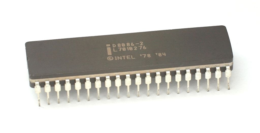
Intel D8086-2 – 16-bit HMOS microprocessor at 8 MHZ
Definition
The D8086-2 is a variant of the 8086 produced by Intel, a 16-bit microprocessor with an external multiplexed address/data bus, intended for microprocessor-based systems with external memory and peripherals on a parallel bus. The “-2” suffix identifies the version with a nominal maximum clock up to 8 MHZ, positioned between the “base” 8086 and the 8086-1.
From an architectural standpoint, the 8086 introduces a segmented model and an internal split into a bus unit and an execution unit, with a prefetch mechanism that improves memory bandwidth utilization compared to strictly sequential execution.

Bus interface unit (BIU) and execution unit (EU): prefetch and instruction queue
Internal functions are logically divided into two blocks:
BIU (bus interface unit): handles instruction fetch, the internal queue, memory/I/O accesses, and address relocation (segmentation).
EU (execution unit): decodes and executes instructions, requesting operands from the BIU and delegating external reads/writes to the BIU.
Practically, the BIU can prefetch instructions while the EU is executing: up to 6 bytes of the instruction stream can be queued, reducing bus idle time and improving perceived performance at the same clock.
Memory organization: 20-bit addressing and 64K segments
The 8086 provides a 20-bit address, so it can directly address up to 1 MB of space (00000h–FFFFFh). Memory is logically organized into segments:
Code, data, extra data, stack: each up to 64 KB.
Segments are aligned on 16-byte boundaries (paragraph boundary).
Memory references are computed as segment base + offset, with segment register selection typically driven by architectural rules.
In practice, this model enables structured and relocatable programs, but it requires careful segment management (especially in assembly or low-level runtimes).
External bus: 16-bit, high/low banks, and even/odd byte handling
Physically, memory is seen as two 8-bit banks:
low bank on D7–D0
high bank on D15–D8
The processor uses A0 and BHE to selectively enable even/odd bytes or a full word. Words can also reside at odd addresses: in that case the BIU performs two external accesses (a performance penalty for word operands; instruction fetch typically occurs as words).
Minimum mode and maximum mode: why two modes exist
The MN/MX pin defines the system mode:
Minimum mode: the 8086 directly generates bus control signals (simple, single-processor systems).
Maximum mode: the 8086 outputs encoded status lines (S0–S2) and an external controller (typically 8288) generates bus commands in a MULTIBUS-style scheme; useful for more complex systems and with coprocessors/other bus masters.
Practically, maximum mode is the typical choice when you want more “modular” configurations (math coprocessor, advanced DMA/bus mastering, more structured architectures).
Key signals and system design
Some signals are central to system design:
ALE to latch the address during T1 (since AD0–AD15 are multiplexed).
READY to insert wait states with slow memories.
HOLD/HLDA (minimum) or RQ/GT (maximum) for bus arbitration with other masters.
LOCK for critical sequences (prevents other masters from taking the bus during sensitive windows).
QS0/QS1 to monitor instruction queue status (useful for debug or external tracking logic).
Sketch of the most important connections
AD15..AD0 (multiplexed address/data) A19..A16 + BHE/A0
┌────────────────────────────────────────────────────────────────────────┐
│ D8086-2 │
│ │
│ AD15..AD0 ────────────────┬───────────────► 8282/8283 (address latches)│
│ │ │
│ └───────────────► 8286/8287 (data transceiver)│
│ │
│ ALE ─────────────────────────► latch enable │
│ RD/WR or (S0..S2 + 8288) ─────► bus controls │
│ READY ───────────────────────► wait states │
│ MN/MX ───────────────────────► minimum / maximum mode │
└────────────────────────────────────────────────────────────────────────┘
│
├────────► memory (RAM/ROM) on 16-bit bus (high/low banks)
└────────► I/O peripherals (read/write I/O cycles)
Table 1 – Identification data and specifications
| Characteristic | Indicative value |
|---|
| Device | Intel D8086-2 |
| Class | 16-bit microprocessor |
| Technology | HMOS (8086 family) |
| Nominal frequency | Up to 8 MHZ (speed grade “-2”) |
| Addressing | 20-bit, up to 1 MB space |
| External data bus | 16-bit (byte control via A0/BHE) |
| External address bus | Up to A19 (with multiplexed AD and external latches) |
| Typical package | 40-pin (DIP/CERDIP and plastic versions) |
| System modes | Minimum mode / maximum mode via MN/MX |
Table 2 – Operational and design considerations
| Aspect | Practical meaning |
|---|
| BIU/EU with prefetch | Better bus utilization: BIU can queue up to 6 bytes of instructions while EU executes |
| 64K segmentation | Code/data/stack structure: powerful but requires correct base+offset management |
| Multiplexed AD lines | Requires external latching (ALE + 8282/8283 or equivalent) to stabilize addresses |
| READY and wait states | Allows the use of slower memories/peripherals without violating timing |
| Minimum vs maximum mode | Minimum: “direct” bus control. Maximum: status + controller (8288) for more complex systems |
| A0/BHE and memory banks | Efficient access for aligned words; penalty on odd-address words (two cycles) |
| LOCK and bus arbitration | Protects critical sequences and reduces contention risk in multi-master systems |