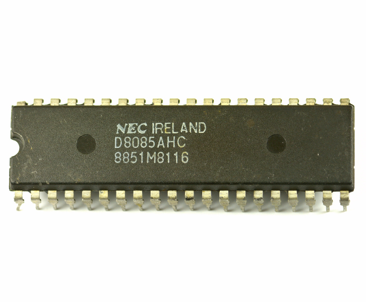
NEC D8085AH CPU plastic version
The 8085 is an 8-bit microprocessor designed by Intel and introduced in the second half of the 1970s as a more “integrated” evolution of the 8080. It is software-compatible with the 8080 at the instruction-set level, but it simplifies system integration thanks to key features: a single +5 V supply, an on-chip clock generator, and built-in interfaces (a richer interrupt system and a simple 1-bit serial interface).
In practice, it is a CPU intended for systems with external RAM/ROM and I/O, on a parallel bus, typical of industrial controllers, instrumentation, and educational/hobby designs.

Bus and addressing: 8-bit data, 16-bit addresses (64 KB)
The 8085 uses:
8-bit data bus.
16-bit address bus, therefore up to 64 KB address space.
AD0–AD7 multiplexed lines (low address + data): during the first phase of the bus cycle they carry the low address, then they become the data bus.
Dedicated A8–A15 lines for the high address.
ALE (address latch enable) to “capture” the low address into an external latch and keep it stable during the data transfer.
Practical consequence: an external latch such as 74LS373/8282 (or equivalent) is almost always used to separate A0–A7 from the data bus.
Power and clock: why the 8085 was easier to integrate
Compared to the 8080 (which required multiple supply voltages), the 8085 operates from a single +5 V supply, reducing regulators and board complexity.
It also integrates a clock generator: with an external crystal or an RC/LC network, the internal clock can be derived without a separate clock generator as in classic 8080 systems. Typical frequencies depend on the speed grade and are on the order of 3–6 MHZ.
Registers and programming model: minimal but effective
The logical model includes:
Accumulator A and the flag register.
General registers B, C, D, E, H, L (also usable as pairs BC, DE, HL).
16-bit PC (program counter) and 16-bit SP (stack pointer).
Practically, the register-pair organization makes pointers and address-oriented operations convenient while remaining in an 8-bit paradigm.
Interrupts and 1-bit serial: event control and simple links
The 8085 adds a more articulated interrupt system, with:
TRAP (non-maskable, highest priority).
RST 7.5, RST 6.5, RST 5.5 (maskable and vectored).
INTR (generic interrupt request, with external acknowledge).
It also includes a minimal 1-bit serial interface:
In practice, SID/SOD are useful for slow signals, simple diagnostics, synchronization, or bit-banged links, without replacing a full UART.
Sketch of the most important connections
                 A8..A15 (high address) + AD7..AD0 (low addr / data)
        ┌──────────────────────────────────────────────────────────┐
        │                         8085                              │
        │  A8..A15 ────────────────────────────────► address bus     │
        │  AD0..AD7 ───────┬───────────────► data bus (D0..D7)       │
        │                  │                                          │
        │  ALE ───────────►│ latch enable                             │
        │                  ▼                                          │
        │             ┌───────────┐                                   │
        │             │  LATCH    │  (e.g., 74LS373/8282)              │
        │             └───────────┘                                   │
        │                  │                                          │
        │                  └──────────────► A0..A7 (low address)       │
        │                                                          │
        │  RD/WR, IO/M ─────────────────► memory/I-O cycle controls   │
        │  TRAP, RST7.5/6.5/5.5, INTR ──► interrupts                  │
        │  SID/SOD ─────────────────────► 1-bit serial                │
        └──────────────────────────────────────────────────────────┘
                         │
                         ├────────► ROM (firmware)
                         ├────────► RAM (data/stack)
                         └────────► I/O (memory-mapped or I/O-mapped)
Table 1 – Identification data and specifications
| Characteristic | Indicative value |
|---|
| Device | 8085 |
| Class | 8-bit microprocessor |
| Introduction | 1976 (first commercial versions) |
| Data bus | 8-bit |
| Address bus | 16-bit (up to 64 KB) |
| Multiplexed lines | AD0–AD7 (A0–A7 / D0–D7) + ALE |
| Supply | Single +5 V |
| Clock | On-chip generator (external crystal/RC/LC) |
| Serial I/O | SID (in), SOD (out) |
| Interrupts | TRAP, RST 7.5, RST 6.5, RST 5.5, INTR |
| Typical package | DIP 40 |
Table 2 – Operational and design considerations
| Aspect | Practical meaning |
|---|
| 8080 compatibility | Easier software migration: 8080 toolchains and code are often reusable |
| Single +5 V | Simpler, lower-cost power design compared to multi-voltage solutions |
| Multiplexed AD0–AD7 | Requires an external latch to hold A0–A7 stable during bus cycles |
| Integrated clock generator | Reduces external components; enables compact designs |
| Vectored interrupts | More structured event handling (priorities and dedicated vectors) |
| SID/SOD | Minimal serial channel for slow signals and service functions |
| “System” architecture | Requires external RAM/ROM and decoding: the memory map is part of the design |
8085 family features :
- Single +5v Power Supply with 10% Voltage margin
- 3 MHz, 5 MHz and 6 MHz Selection Available
- 1,3 us Instrucion Cycle (8085AH); 0,8 us (8085AH-2), 0,67 us (8087AH-1)
- 100% Software Compatible with 8080A
- On-Chip Clock Generator with External Crystal, LC or RC Network
- On-Chip System Controller ; Advanced Cycle Status Informatio Available for Large System Control
- Four Vectored Interrupt Inputs (One Is non Maskable) Plus an 8080A Compatible Interrupt
- Serial in/Serial Out Port
- Decimal, Binary and Double Precision Arithmetic
- Direct addressing Capability to 64k Bytes of Memory