D4-6901-5 / D4-6900-5 – complex Harris chipset for DEC in the DCJ11-AC module (DC335 + DC334) for the PDP-11 architecture
Definition
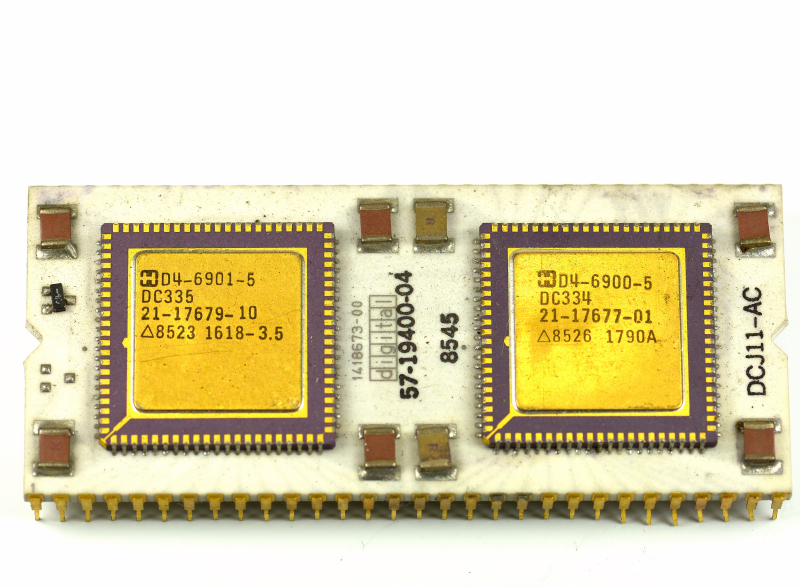
The D4-6901-5 and D4-6900-5 are a complex chipset produced by Harris Corporation for Digital Equipment Corporation. The component was fitted into the DCJ11-AC module and consisted of two main chips identified as DC335 and DC334.
Together, they implement CPU and control functions typical of PDP-11 systems, combining decode/control logic (PLA/ROM and Q logic) with the “core” side tied to architectural registers, machine state (PSW), arithmetic, and the memory/bus interface.
The stated operating characteristics for use on PDP-11 systems are: 4.5 MHZ frequency, a 32-bit data bus, and approximately 120,000 transistors overall.

Two-chip structure: roles of DC335 and DC334
Within the DCJ11-AC module, the function split follows a classic “control + datapath” approach: one chip is more control/decode oriented, the other is closer to registers/arithmetic/external interfacing.
DC335: PLA/ROM control and decode start (Q logic)
The DC335 chip primarily controlled:
ROM/PLA resources, including a 512 × 25-bit PLA and a 768 ROM.
The start of PLA decode through Q logic, i.e., the initial phase of interpreting/initiating control sequences.
Other interface functions, related to signal handling and cooperation with the other chip in the module.
Practically, DC335 concentrates the “orchestration” and decode/control portion needed to drive the instruction machine and state transitions correctly.
DC334: PDP-11 registers, PSW, 32-bit arithmetic, memory and interfaces
The DC334 chip primarily controlled:
The PDP-11 general architectural registers at 16-bit width.
The PSW (processor status word), i.e., processor state (flags and execution control).
All 32-bit arithmetic functions, providing wider numeric processing than the architectural word size.
Memory control and the external interface, handling signals and bus interaction.
Instruction prefetch logic, useful for reducing wait time between fetch and decode/execute.
Additional interface functions to complete the module as an integrated “CPU package”.
Practically, DC334 is the part closest to what software “sees” as the CPU: registers, state, arithmetic, and the connection to system memory/I/O.
System parameters: frequency, bus width, and complexity
Frequency: 4.5 MHZ
A 4.5 MHZ frequency is consistent with minicomputer/embedded platforms of the era, where real-world performance depends heavily on the combination of decode, prefetch, and memory latency.
Data bus: 32-bit
The 32-bit data bus is a key element: it increases transfer capability and allows the memory/I-O subsystem to feed internal operations more efficiently (especially 32-bit operations).
Transistors: 120,000
A total of approximately 120,000 transistors indicates a high integration level for a two-chip module: sufficient to include control logic, registers, an arithmetic datapath, and interfaces in a compact implementation.
Sketch of the most important connections
                 system bus + memory/I-O (PDP-11 platform)
        ┌──────────────────────────────────────────────────────────┐
        │     RAM/ROM, peripherals, interrupts, timing, controllers │
        └───────────────────────────────┬──────────────────────────┘
                                        │ 32-bit data bus
                                        ▼
                           ┌─────────────────────────────┐
                           │   D4-6901-5 / D4-6900-5      │
                           │   DCJ11-AC module            │
                           │   4.5 MHZ                    │
                           └─────────────┬───────────────┘
                                         │
                     ┌───────────────────┴───────────────────┐
                     ▼                                       ▼
          ┌──────────────────────┐                ┌──────────────────────┐
          │ DC335 (control)      │                │ DC334 (core)         │
          │ PLA 512×25 + ROM 768 │                │ PDP-11 regs 16-bit    │
          │ Q logic (start decode)│               │ PSW                   │
          │ interfaces           │                │ 32-bit arithmetic     │
          └──────────────────────┘                │ memory + interfaces   │
                                                  │ instruction prefetch  │
                                                  └──────────────────────┘
Table 1 – Identification data and specifications
| Characteristic | Indicative value |
|---|
| Device | D4-6901-5 / D4-6900-5 |
| Manufacturer | Harris (for DEC) |
| Insertion module | DCJ11-AC |
| Target architecture | PDP-11 |
| Composition | Two chips: DC335 + DC334 |
| Frequency | 4.5 MHZ |
| Data bus | 32-bit |
| Transistors | 120,000 |
Table 2 – Functional split: DC335 vs DC334
| Aspect | Practical meaning |
|---|
| DC335: PLA/ROM | Implements control resources (512×25-bit PLA, ROM 768) and supports control-sequence signal generation |
| DC335: Q logic | Starts PLA decode and coordinates the first phases of interpretation/control |
| DC334: registers + PSW | Manages architectural registers (16-bit) and machine state via the PSW |
| DC334: 32-bit arithmetic | Executes 32-bit operations, improving compute capability and data handling |
| DC334: memory and interfaces | Connects the CPU to memory and the external bus, including instruction prefetch to reduce waits |
| Two-chip architecture | Control/datapath separation: more scalable and verifiable, integrating complex functions into the module |