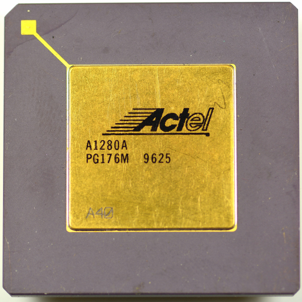
ACTEL A1280
Definition
The Actel A1280 is an FPGA in the ACT 2 family, based on ANTIFUSE PLICE technology: a grid-based programmable-logic device that allows implementing custom digital hardware (combinational logic, sequential logic, state machines, interfaces, small datapaths) using synthesis and place-and-route tools.
Unlike SRAM-configured FPGA devices, the A1280 (ACT 2) is ONE-TIME PROGRAMMABLE (OTP): once programmed, the configuration is NON-VOLATILE and the circuit is operational immediately at power-up (no bitstream load from external memory after power-on).

Programming technology: ANTIFUSE PLICE (OTP, NON-VOLATILE)
The key principle is the use of ANTIFUSE elements (PLICE): during programming, permanent connections are “closed” at the required points in the internal routing. This means:
The configuration is permanent and resilient to power interruptions.
No configuration boot is required (no dedicated SPI FLASH just for the bitstream, in typical systems).
Reprogramming is not supported (except by replacing the chip).
Historically, this architectural choice is valued in applications where reliability, robustness, and copy protection matter (reverse engineering is more difficult than with loadable solutions).
Internal architecture (ACT 2: C-MODULE AND S-MODULE)
The ACT 2 family uses an architecture with two module types:
These modules are connected through a channeled routing network programmed via antifuse. The practical goal is predictable performance and good utilization, supported by automatic placement and routing tools.
Main device resources (A1280A class)
In terms of capacity, the A1280 (ACT 2) sits in the historical “mid-range” of the family, featuring:
Indicative density of about 8,000 gates (typical metric of the era).
About 1,232 LOGIC MODULES total, split between S-MODULE and C-MODULE.
Up to 140 user I/O (package-dependent).
A large number of antifuse (PLICE) elements to implement internal connections and routing.
In practice, it is suitable for system logic, complex glue logic, “simple” parallel/serial interfaces, decoding, control, and small pipelines where deterministic latency is useful.
Performance and timing (what really matters)
On these families, real performance depends heavily on:
Logic depth (number of LUT-equivalent levels implemented in C-MODULE).
Routing length and congestion (delays dominate in high-fanout designs).
Pipelining choices (registering signals with flip-flops to increase FMAX).
Clock constraints and floorplan quality (even with automatic tools, constraints remain critical).
A practical rule: to increase usable frequency, it helps to split logic into registered stages (pipeline) and reduce fanout and long paths.
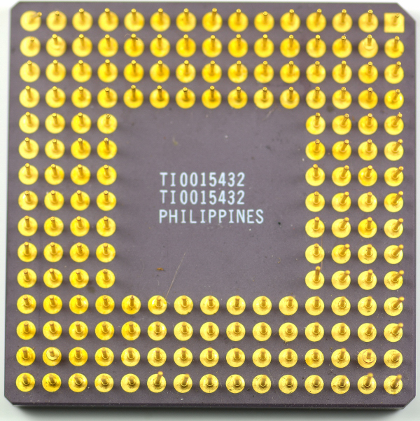
Packaging and board integration
The A1280 has been available in multiple packages (plastic and ceramic) with different pin counts: the actual availability of I/O and dedicated signals depends on the chosen package. In many designs, package choice is driven by:
Required number of I/O and target electrical standards.
Layout constraints (QFP vs PGA, height, inspectability).
Temperature grade (commercial/industrial/military) and reliability requirements.
Development flow (how an A1280 is designed)
The typical flow is the classic FPGA flow:
Description in HDL (VHDL/VERILOG) or schematic entry (historically common).
Synthesis into a netlist.
Automatic place-and-route with timing constraints.
Post-route timing analysis and simulation.
OTP programming of the device via programmer/toolchain support (after that, the chip is “final”).
Sketch of the most important connections
                 ┌──────────────────────────────┐
                 │           HOST SYSTEM         │
                 │ CPU/MCU + BUS + PERIPHERALS   │
                 └──────────────┬───────────────┘
                                │ digital I/O (data/address/control)
                                ▼
                       ┌──────────────────┐
                       │    ACTEL A1280   │
                       │       FPGA       │
                       │ C-MODULE/S-MODULE│
                       │ ANTIFUSE ROUTING │
                       └───────┬──────────┘
                               │ signals to the rest of the board
                               ▼
                 ┌────────────────────────────────┐
                 │ EXTERNAL MEMORIES / I/O / LOGIC │
                 │ buffers, latches, transceivers, │
                 │ etc                             │
                 └────────────────────────────────┘

Programming (before deployment or during production):
                 ┌──────────────────┐
                 │ PROGRAMMER /     │
                 │ TOOL INTERFACE   │
                 └───────┬──────────┘
                         │ programming connection (factory setup)
                         ▼
                    [A1280 (OTP)]
Table 1 – Identification data and specifications (English)
| Characteristic | Typical value |
|---|
| Device | Actel A1280 (ACT 2 family) |
| Type | FPGA based on ANTIFUSE (PLICE) |
| Programming | OTP, NON-VOLATILE configuration |
| Logic density | ~ 8,000 gates |
| Logic modules | ~ 1,232 LOGIC MODULES (with S-MODULE and C-MODULE) |
| Flip-flops (max) | ~ 998 |
| User I/O (max) | ~ 140 (package-dependent) |
| Process/technology | CMOS (ACT 2 family) |
| Package (family-typical) | PLCC/QFP/PGA/CQFP options depending on variant and availability |
Table 2 – Operational and design aspects (English)
| Aspect | Practical meaning |
|---|
| Startup | “Instant-on”: no bitstream loading after power-on |
| Updatability | Not reprogrammable in the field (OTP device) |
| Timing | Strongly depends on routing and fanout; pipelining recommended to increase FMAX |
| Reliability | Permanent configuration, robust to power loss |
| Security | Configuration is not easily extractable compared to loadable solutions |
| Typical use | Glue logic, interfaces, control, decoding, small datapaths/pipelines |
| Toolchain | Synthesis + place-and-route + timing analysis + OTP programming |