

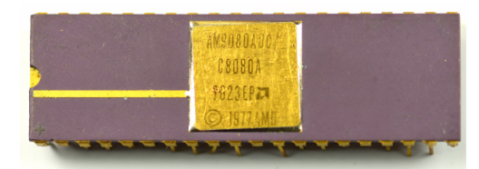
AMD AM9080ADC – 8-bit 8080A-compatible microprocessor, NMOS technology and typical 2 MHZ clock
Definition
The AM9080 (often also listed as AM9080A) is an 8-bit CPU produced by AMD as a compatible implementation of the Intel 8080/8080A. In the second half of the 1970s—and in the stated timeframe (1977)—this component belongs to the industrial “second source” context: equivalent devices used to ensure availability, supply continuity, and alternatives for military/industrial markets.
The manufacturing technology is NMOS (n-channel silicon-gate MOS) and the most typical nominal frequency for the base variants is 2 MHZ.
Compatibility with Intel 8080/8080A and the licensed context
The AM9080 was designed as an 8080/8080A-compatible CPU, with the same overall approach: external buses, control signals, and programming model. In those years, “second sourcing” arrangements with Intel were formalized, which mattered for adoption in markets that would not accept a single-supplier component.
Practically, compatibility means that a board designed for an 8080A can be adapted with minimal changes, especially when clock/timing and power rails are already “8080-style”.
Bus and addressing: 8-bit data, 16-bit addresses (64 KB)
The AM9080A uses an 8-bit data bus and a 16-bit address bus, therefore it can address up to 64 KB. It is intended for systems with external memory and peripherals: ROM for firmware, RAM for data/stack, and parallel-bus I/O through address decoding logic.
In typical late-1970s designs, the memory map and chip-select logic (RAM/ROM/I-O) are integral to the design and define the overall board architecture.
NMOS technology and “8080-style” power rails
As an 8080A-derived design in NMOS technology, integration follows the era’s philosophy, including the multi-rail supply typical of the 8080 family: +5 V, +12 V, and −5 V for internal domains and bias conditions.
Practically, this distinguishes these systems from later, more “integrated” microprocessors (for example the 8085 and 6502), which tend to simplify power requirements and surrounding hardware.
System signals and handshake: READY/WAIT and bus control
The AM9080A exposes control signals that make interfacing to memories and I/O devices of different speeds easier:
The READY signal allows slow devices to be supported by inserting waits, while WAIT represents the bus wait condition when a device is not ready. Signals such as DBIN (data bus in), WR (write), and synchronization lines help define the type of cycle (read/write) and the timing of the transfer.
This is especially useful in systems with heterogeneous peripherals, where part of the bus can be slower than main RAM or boot ROM.
Sketch of the most important connections
                 A0..A15 (addresses) + D0..D7 (data) + bus control
        ┌──────────────────────────────────────────────────────────┐
        │                  address decode / glue logic              │
        │   ROM/RAM/I-O chip selects + READY/WAIT handling          │
        └───────────────────────────┬──────────────────────────────┘
                                    │
                                    ▼
                         ┌────────────────────────┐
                         │       AMD AM9080A       │
                         │      8-bit NMOS CPU     │
                         │  A0..A15   D0..D7        │
                         │  DBIN, WR, READY, WAIT   │
                         │  RESET, INT, HOLD/HLDA   │
                         └───────────┬─────────────┘
                                     │
                                     ├────────► ROM (firmware)
                                     ├────────► RAM (data/stack)
                                     └────────► I/O (parallel-bus interfaces)
Table 1 – Identification data and specifications
| Characteristic | Indicative value |
|---|---|
| Device | AMD AM9080 / AM9080A |
| Class | 8-bit microprocessor compatible with 8080/8080A |
| Year stated in context | 1977 (production/use during the 8080A era) |
| Technology | NMOS (n-channel silicon-gate MOS) |
| Typical clock | 2 MHZ (higher family variants also existed) |
| Data bus | 8-bit |
| Address bus | 16-bit (up to 64 KB) |
| Typical supplies | +5 V, +12 V, −5 V (8080A-style) |
| Common package | DIP 40 |
Table 2 – Operational and design considerations
| Aspect | Practical meaning |
|---|---|
| Second source | Reduces supply-chain risk and supports “no single source” adoption requirements |
| 1970s NMOS | Power and multi-rail constraints; heavier power design than later CPUs |
| 64 KB address space | Sufficient for compact systems: boot ROM + RAM + mapped I/O |
| READY/WAIT handshake | Enables slow memories/peripherals without redesigning the entire timing scheme |
| External-bus architecture | Robustness and performance depend strongly on address decoding and glue logic |
| 8080A compatibility | Reuse of toolchains and concepts (monitor software, firmware, parallel-bus I/O) |