

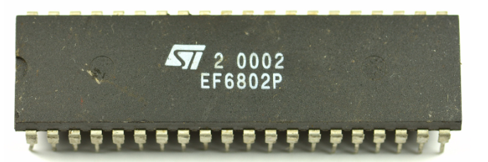
ST EF6802
The ST EF6802 is an 8-bit CPU in the 6802 class, positioned as an evolution/successor to the 6800, maintaining software compatibility with the EF6800 line while adding integration features that are useful for more compact embedded systems. The distinguishing elements are the on-chip clock circuit and 128 × 8-bit on-chip RAM, with a 32-byte retainable portion, which reduce external component count and improve state handling under specific operating conditions.
In practice, EF6802 aims to simplify board design (fewer parts, fewer critical traces) while keeping a programming model close to that of the 6800.
From the 6800 to the 6802: what really changes
Successor to the 6800
The 6802 was introduced to provide a more integrated platform than the 6800: instead of relying entirely on external clock generation and minimal external RAM, it brings basic resources onto the chip, making it easier to build “minimal” but complete systems.
EF6800 compatibility
Software compatibility with EF6800 allows reuse of firmware, assembly routines, and control logic already developed for the family, reducing porting time and integration risk.
On-chip clock: integration and platform robustness
On-chip clock circuit
The integrated clock circuit makes it possible to:
reduce external clock-related components
simplify PCB layout (fewer sensitive clock lines)
increase timing repeatability in production
Operationally, this is an advantage in industrial electronics and instrumentation, where clock stability and robustness can matter as much as raw performance.
On-chip RAM: 128 × 8-bit and 32 retainable bytes
128 × 8 bit on-chip RAM
The 128-byte internal RAM is useful for:
critical variables kept “close” to the core
stack and counters in compact systems
small buffers without latency penalties
32 bytes of RAM are retainable
The 32-byte retainable portion can preserve a minimal set of information (state, flags, counters, parameters) under operating conditions defined by the platform’s power/backup design. In practice, it provides a “state nucleus” useful for controlled restarts or for retaining context in duty-cycled systems.
Expandability: up to 64K and 16-bit addressing
Expandable to 64K words
The CPU is expandable up to 64K of addressable space, consistent with:
16 bit memory addressing
16-bit addressing enables a memory map up to 64 KB. Operationally:
ROM (firmware), RAM (data), and peripherals can be memory-mapped
address decoding is central to system stability (ROM/RAM/I/O windows)
TTL-compatible I/O: simplified interfacing
Standard TTL-compatible inputs and outputs
TTL compatibility makes integration easier with:
latches, decoders, drivers, and standard logic
classic parallel buses and peripherals of the era
In practice, it reduces the need for level shifting and simplifies the BOM.
8-bit word size and interrupts
8 bit word size
The CPU natively operates on bytes, with instructions oriented to control, logic, and 8-bit arithmetic.
Interrupt capability
Interrupt support enables asynchronous event handling (timers, I/O, faults, communications) without constant polling, improving responsiveness and firmware determinism.
Versions: 1 MHZ and 1.5 MHZ
Versions: 1 MHZ, 1.5 MHZ
Versions at 1 MHZ and 1.5 MHZ are specified. In practice, the speed grade is selected based on:
required performance
timing compatibility with memories/peripherals
power and thermal constraints
Sketch of the most important connections
                 16-bit address bus + 8-bit data bus + control
        ┌──────────────────────────────────────────────────────────┐
        │              system logic / decoding                      │
        │  ROM (firmware), optional external RAM, I/O, interrupts   │
        └───────────────────────────────┬──────────────────────────┘
                                        │
                                        ▼
                           ┌─────────────────────────────┐
                           │            ST EF6802         │
                           │   6802 CPU (6800 successor)  │
                           │   on-chip clock              │
                           │   on-chip RAM 128×8          │
                           │   32 retainable bytes        │
                           └─────────────┬───────────────┘
                                         │
                                         ├────────► external memory (up to 64K, if used)
                                         └────────► TTL-compatible I/O and interrupts
Table 1 – Identification data and specifications
| Characteristic | Indicative value |
|---|---|
| Device | ST EF6802 |
| Class | 6802 CPU (successor to the 6800) |
| Word size | 8-bit |
| Memory addressing | 16-bit |
| Expandable space | Up to 64K |
| Clock | On-chip clock circuit |
| On-chip RAM | 128 × 8-bit |
| Retainable RAM | 32 bytes |
| Software compatibility | EF6800 (software compatible) |
| I/O | TTL-compatible inputs/outputs |
| Interrupts | Interrupt support |
| Frequency versions | 1 MHZ, 1.5 MHZ |
Table 2 – Operational and design considerations
| Aspect | Practical meaning |
|---|---|
| Successor to the 6800 | More integration (clock + RAM) with ecosystem continuity |
| On-chip clock | Reduces external parts and simplifies compact board integration |
| 128-byte internal RAM | Local variables/stack with reduced latency; useful in minimal systems |
| 32-byte retainable | Preserves minimal state (parameters/flags) under specific operating conditions |
| EF6800 compatibility | Toolchain/firmware reuse and easier porting |
| 64K addressable | Platform scalability with ROM/RAM and memory-mapped peripherals |
| TTL-compatible I/O | Simple interfacing with standard logic and classic peripherals |
| Interrupts | Event handling without constant polling and more responsive firmware |
| 1–1.5 MHZ | Speed-grade choice based on performance and system constraints |