

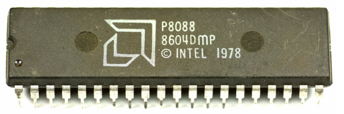
AMD P8088
The 8088 is an x86-family microprocessor designed to keep a 16-bit internal core (compatibility and programming model aligned with the 8086), while using an 8-bit external data-bus interface. This architectural choice reduces overall system complexity (cheaper memories and peripherals, fewer support components), at the cost of lower memory-transfer performance compared to a CPU with a 16-bit external data bus.
It was produced by Intel and is known for adoption in many personal and embedded systems of the late 1970s and 1980s, including early PC platforms built around 8-bit buses.
Base architecture: 16-bit internal core, 8-bit external data bus
The stated 8088-series characteristics reaffirm the two core points:
8-bit data bus interface: an 8-bit external interface, so many 16-bit transfers occur in two bus cycles.
16-bit internal architecture: the ALU and registers operate natively on 16-bit words.
In practice, this makes the 8088 ideal for platforms with 8-bit RAM and I/O (simpler and cheaper), but it penalizes throughput on workloads that depend heavily on memory bandwidth.
Addressing: up to 1 MB and the segmented model
The 8088 provides direct addressing capability up to 1 Mbyte thanks to a 20-bit address bus. The memory model remains the segmented one:
Physical address generated by combining segment and offset.
Logical separation of code, data, and stack via segment registers.
In practice, segmentation enables flexible memory maps, but increases software complexity (pointer handling, linker/locator behavior, and memory conventions).
Direct software compatibility with the 8086
The 8088 series is specified as directly software compatible with the 8086 CPU. Operationally this means:
The same instruction set and the same basic programming model.
High portability of 8086 software, with differences mainly in performance due to the 8-bit external bus and platform timing.
Register set and addressing modes: “16-bit-class” richness
14-word by 16-bit register set with symmetrical operations
The CPU is described as having a 14-word by 16-bit register set with symmetrical operations. Practically, this reflects a comparatively rich register and segmentation model for the era, combining general-purpose registers and segment registers to handle code/data/stack and pointers with more flexibility than many pure 8-bit CPUs.
24 operand addressing modes
The 24 operand addressing modes expand how operands can be referenced in memory and registers. Practically, this helps compilers and optimized assembly, reducing “glue” instructions for address calculations and structured data access.
Byte, word, and block operations
The CPU supports operations on bytes, words, and blocks. Operationally, block operations are central for memory moves/copies and system routines, improving throughput and producing more compact code for buffer transfers and string handling.
8-bit and 16-bit signed/unsigned arithmetic, binary and decimal, including multiply and divide
The series supports:
Signed and unsigned arithmetic at 8-bit and 16-bit widths.
Binary or decimal formats (in practice, BCD-related instruction/flag behavior).
Multiply and divide operations.
Practical implication: the 8088 is not limited to basic add/subtract; it includes more complex operations that reduce long software routines, especially in business/management computing, calculations, and conversions.
Prefetch and instruction queue: practical performance impact
The 8088 uses an instruction prefetch queue (typically 4 bytes) to overlap instruction fetch with decode/execute.
In practice:
On linear flows, prefetch can reduce stalls and improve throughput.
On code with frequent branches or on slow-memory platforms, the queue empties more often and the benefit is reduced.
Clock: 8088 vs 8088-2
Two clock rates are stated:
5 MHZ for the 8088.
8 MHZ for the 8088-2.
In practice, higher frequency increases potential throughput, but real performance still depends on the memory subsystem and any wait states imposed by the chipset/system logic.
Variants and operating conditions: EXPRESS, temperature ranges
Available in EXPRESS
The EXPRESS wording should be understood as availability within a specific supply/program or commercial selection line.
Standard temperature range and extended temperature range
Availability in standard and extended temperature ranges implies versions targeted at industrial or harsher environments. Practically, “extended” variants are relevant for industrial electronics and systems with stricter environmental constraints.
System interface: multiplexed bus and control signals
Like many CPUs of its generation, the 8088 uses multiplexed lines to reduce pin count:
Some lines carry addresses in one phase of the bus cycle and data in another, requiring external latches to hold the address.
Control signals exist for memory and I/O reads/writes and for interrupt/DMA coordination through system logic.
In practice, a typical platform includes latches, transceivers, and a bus controller/chipset (or TTL glue logic) that define timing, wait states, and the I/O map.
Typical deployments and historical context
The 8088 was chosen in many platforms because it balanced:
16-bit programming compatibility.
“8-bit bus” costs at the memory and peripheral level.
It is historically associated with early IBM PCs and with many industrial systems using legacy peripherals and simple buses.
Sketch of the most important connections
                 20-bit address bus + 8-bit data bus + control
        ┌──────────────────────────────────────────────────────────┐
        │              system logic / chipset                       │
        │  address latches, transceivers, decoding, wait-states, DMA │
        └───────────────────────────────┬──────────────────────────┘
                                        │
                                        ▼
                           ┌─────────────────────────────┐
                           │             8088            │
                           │   16-bit core, 8-bit data bus│
                           │   20-bit address bus         │
                           │   prefetch queue (4 bytes)   │
                           └─────────────┬───────────────┘
                                         │
                                         ├────────► ROM/BIOS and program memory
                                         ├────────► RAM (data/stack)
                                         └────────► I/O (devices in I/O space or memory-mapped)
Table 1 – Identification data and specifications
| Characteristic | Indicative value |
|---|---|
| Device | 8088 |
| Manufacturer | Intel |
| Class | x86 CPU with 16-bit internal architecture |
| External data bus | 8-bit |
| Address bus | 20-bit |
| Addressable space | 1 MB |
| Software compatibility | 8086-compatible (direct software compatibility) |
| Register set | 14 words × 16-bit (register and segment set) |
| Addressing modes | 24 operand addressing modes |
| Data operations | Byte, word, and block operations |
| Arithmetic | 8/16-bit signed/unsigned, binary or decimal, including multiply and divide |
| Prefetch | Instruction queue (typically 4 bytes) |
| Clock | 5 MHZ (8088), 8 MHZ (8088-2) |
| Operating variants | Available in EXPRESS; standard and extended temperature ranges |
Table 2 – Operational and design considerations
| Aspect | Practical meaning |
|---|---|
| 8-bit external bus with 16-bit core | Lower-cost systems, but word transfers often require two bus cycles |
| 1 MB segmentation model | Flexible memory layout, but higher software complexity (pointers and linking) |
| 24 addressing modes | More flexible operand access; helps compilers and optimization |
| Block operations | More efficient memory moves and more compact code for system routines |
| Multiply/divide arithmetic | Reduces software routines and accelerates calculations vs simpler ALUs |
| Prefetch queue | Improves throughput on linear flows; less effective with many branches or slow memory |
| Multiplexed bus | Fewer pins, but requires latches and glue logic to separate address/data phases |
| Extended temperature range | Better suited to industrial electronics and harsh environments |